| Citation: | Yuanyuan Zhao, Qiurui Wang, Yinping Teng, Zhe Xin, Yusheng Cao, Jialong Duan, Qiyao Guo, Yingli Wang, Qunwei Tang. Strain management in perovskite solar cells[J]. Energy Lab, 2023, 1(3): 230004. doi: 10.54227/elab.20230004 |
Strain management in perovskite solar cells
-
Abstract
Perovskite solar cells (PSCs) currently hold the record for highest power conversion efficiency (PCE) at an impressive 26.1%. However, the state-of-the-art PCEs still fall below theoretical limits, and the long-term stability remains a critical concern for practical implementation of PSCs. Due to the soft ionic nature of metal halide perovskites, the inevitable strain effect on perovskite films has been found to be a key factor in determining both efficiency and stability. In this review, we summarize the recent advancements on the origins of strain, the characterization methodologies, and the impact of strain on perovskite films, as well as various strategies employed to regulate strain and enhance the intrinsic performance of perovskites and solar cells. Our intention is to facilitate scientists with an exhaustive comprehension of the strain effect, and stimulate research endeavors in strain management aimed at enhancing device performance and commercialization.
-
Keywords:
- Perovskite solar cells /
- Strain /
- Stability /
- Power conversion efficiency /
- Carrier recombination
-

-
References
1. W. Zhang, Y. Chao, S. Guo, Energy Lab, 2023, 1, 220004 2. S. Liu, S. Yin, L. Cui, H. Yu, K. Deng, Z. Wang, Y. Xu, L. Wang, H. Wang, Energy Lab, 2023, 1, 220005 3. G. E. Eperon, S. D. Stranks, C. Menelaou, M. B. Johnston, L. M. Herz, H. J. Snaith, Energy & Environmental Science, 2014, 7, 982 4. S. De Wolf, J. Holovsky, S. J. Moon, P. Loper, B. Niesen, M. Ledinsky, F. J. Haug, J. H. Yum, C. Ballif, The Journal of Physical Chemistry Letters, 2014, 5, 1035 5. L. M. Herz, ACS Energy Letters, 2017, 2, 1539 6. S. D. Stranks, G. E. Eperon, G. Grancini, C. Menelaou, M. J. Alcocer, T. Leijtens, L. M. Herz, A. Petrozza, H. J. Snaith, Science, 2013, 342, 341 7. https://www.nrel.gov/pv/interactive-cell-efficiency.html (accessed: October, 2023) 8. M. I. Saidaminov, J. Kim, A. Jain, R. Quintero-Bermudez, H. Tan, G. Long, F. Tan, A. Johnston, Y. Zhao, O. Voznyy, E. H. Sargent, Nature Energy, 2018, 3, 648 9. J. Wu, S. C. Liu, Z. Li, S. Wang, D. J. Xue, Y. Lin, J. S. Hu, National Science Review, 2021, 8, nwab047 10. T. W. Jones, A. Osherov, M. Alsari, M. Sponseller, B. C. Duck, Y.-K. Jung, C. Settens, F. Niroui, R. Brenes, C. V. Stan, Y. Li, M. Abdi-Jalebi, N. Tamura, J. E. Macdonald, M. Burghammer, R. H. Friend, V. Bulović, A. Walsh, G. J. Wilson, S. Lilliu, S. D. Stranks, Energy & Environmental Science, 2019, 12, 596 11. M. V. Khenkin, E. A. Katz, A. Abate, G. Bardizza, J. J. Berry, C. Brabec, F. Brunetti, V. Bulović, Q. Burlingame, A. Di Carlo, R. Cheacharoen, Y.-B. Cheng, A. Colsmann, S. Cros, K. Domanski, M. Dusza, C. J. Fell, S. R. Forrest, Y. Galagan, D. Di Girolamo, M. Grätzel, A. Hagfeldt, E. von Hauff, H. Hoppe, J. Kettle, H. Köbler, M. S. Leite, S. Liu, Y.-L. Loo, J. M. Luther, C.-Q. Ma, M. Madsen, M. Manceau, M. Matheron, M. McGehee, R. Meitzner, M. K. Nazeeruddin, A. F. Nogueira, Ç. Odabaşı, A. Osherov, N.-G. Park, M. O. Reese, F. De Rossi, M. Saliba, U. S. Schubert, H. J. Snaith, S. D. Stranks, W. Tress, P. A. Troshin, V. Turkovic, S. Veenstra, I. Visoly-Fisher, A. Walsh, T. Watson, H. Xie, R. Yıldırım, S. M. Zakeeruddin, K. Zhu, M. Lira-Cantu, Nature Energy, 2020, 5, 35 12. J. A. Steele, H. Jin, I. Dovgaliuk, R. F. Berger, T. Braeckevelt, H. Yuan, C. Martin, E. Solano, K. Lejaeghere, S. M. J. Rogge, C. Notebaert, W. Vandezande, K. P. F. Janssen, B. Goderis, E. Debroye, Y.-K. Wang, Y. Dong, D. Ma, M. Saidaminov, H. Tan, Z. Lu, V. Dyadkin, D. Chernyshov, V. Van Speybroeck, E. H. Sargent, J. Hofkens, M. B. J. Roeffaers, Science, 2019, 365, 679 13. J. Zhao, Y. Deng, H. Wei, X. Zheng, Z. Yu, Y. Shao, J. E. Shield, J. Huang, Science Advances, 2017, 3, eaao5616 14. N. N. Som, P. M. W. P. Sampath, S. D. Dabhi, V. Mankad, S. Shinde, M. L. C. Attygalle, P. K. Jha, Solar Energy, 2018, 173, 1315 15. D. J. Xue, Y. Hou, S. C. Liu, M. Wei, B. Chen, Z. Huang, Z. Li, B. Sun, A. H. Proppe, Y. Dong, M. I. Saidaminov, S. O. Kelley, J. S. Hu, E. H. Sargent, Nature Communications, 2020, 11, 1514 16. Y. Chen, Y. Lei, Y. Li, Y. Yu, J. Cai, M. H. Chiu, R. Rao, Y. Gu, C. Wang, W. Choi, H. Hu, C. Wang, Y. Li, J. Song, J. Zhang, B. Qi, M. Lin, Z. Zhang, A. E. Islam, B. Maruyama, S. Dayeh, L. J. Li, K. Yang, Y. H. Lo, S. Xu, Nature, 2020, 577, 209 17. G. Liu, L. Kong, J. Gong, W. Yang, H. k. Mao, Q. Hu, Z. Liu, R. D. Schaller, D. Zhang, T. Xu, Advanced Functional Materials, 2016, 27, 1604208 18. S. Jiang, Y. Fang, R. Li, H. Xiao, J. Crowley, C. Wang, T. J. White, W. A. Goddard, 3rd, Z. Wang, T. Baikie, J. Fang, Angewandte Chemie International Edition, 2016, 55, 6540 19. H. Yu, Q. Sun, T. Zhang, X. Zhang, Y. Shen, M. Wang, Materials Today Energy, 2021, 19, 100601 20. J. H. Im, C. R. Lee, J. W. Lee, S. W. Park, N. G. Park, Nanoscale, 2011, 3, 4088 21. Y. Fu, H. Zhu, Chen. J, M. P. Hautzinger, X. Zhu, S. J, Nature Reviews Materials, 2019, 4, 169 22. Y. Jiao, S. Yi, H. Wang, B. Li, W. Hao, L. Pan, Y. Shi, X. Li, P. Liu, H. Zhang, C. Gao, J. Zhao, J. Lu, Advanced Functional Materials, 2020, 31, 2006243 23. Y. Dang, Y. Liu, Y. Sun, D. Yuan, X. Liu, W. Lu, G. Liu, H. Xia, X. Tao, CrystEngComm, 2015, 17, 665 24. N. K. McKinnon, D. C. Reeves, M. H. Akabas, Journal of General Physiology, 2011, 138, 453 25. G. Kim, H. Min, K. S. Lee, D. Y. Lee, S. M. Yoon, S. I. Seok, Science, 2020, 370, 108 26. X. Zheng, C. Wu, S. K. Jha, Z. Li, K. Zhu, S. Priya, ACS Energy Letters, 2016, 1, 1014 27. W. Travis, E. N. K. Glover, H. Bronstein, D. O. Scanlon, R. G. Palgrave, Chemical Science, 2016, 7, 4548 28. D. Liu, W. Zha, Y. Guo, R. Sa, ACS Omega, 2020, 5, 893 29. J.-H. Lee, N. C. Bristowe, J. H. Lee, S.-H. Lee, P. D. Bristowe, A. K. Cheetham, H. M. Jang, Chemistry of Materials, 2016, 28, 4259 30. L.-J. Ji, S.-J. Sun, Y. Qin, K. Li, W. Li, Coordination Chemistry Reviews, 2019, 391, 15 31. Q. A. Akkerman, L. Manna, ACS Energy Letters, 2020, 5, 604 32. R. J. Sutton, M. R. Filip, A. A. Haghighirad, N. Sakai, B. Wenger, F. Giustino, H. J. Snaith, ACS Energy Letters, 2018, 3, 1787 33. B. Wang, N. Novendra, A. Navrotsky, Journal of the American Chemical Society, 2019, 141, 14501 34. F. Bertolotti, L. Protesescu, M. V. Kovalenko, S. Yakunin, A. Cervellino, S. J. L. Billinge, M. W. Terban, J. S. Pedersen, N. Masciocchi, A. Guagliardi, ACS Nano, 2017, 11, 3819 35. C. Zhu, X. Niu, Y. Fu, N. Li, C. Hu, Y. Chen, X. He, G. Na, P. Liu, H. Zai, Y. Ge, Y. Lu, X. Ke, Y. Bai, S. Yang, P. Chen, Y. Li, M. Sui, L. Zhang, H. Zhou, Q. Chen, Nature Communications, 2019, 10, 815 36. I. Mela, C. Poudel, M. Anaya, G. Delport, K. Frohna, S. Macpherson, T. A. S. Doherty, A. Scheeder, S. D. Stranks, C. F. Kaminski, Advanced Functional Materials, 2021, 31, 2100293 37. S. Jariwala, H. Sun, G. W. P. Adhyaksa, A. Lof, L. A. Muscarella, B. Ehrler, E. C. Garnett, D. S. Ginger, Joule, 2019, 3, 3048 38. D. Liu, D. Luo, A. N. Iqbal, K. W. P. Orr, T. A. S. Doherty, Z. H. Lu, S. D. Stranks, W. Zhang, Nature Materials, 2021, 20, 1337 39. N. Rolston, K. A. Bush, A. D. Printz, A. Gold-Parker, Y. Ding, M. F. Toney, M. D. McGehee, R. H. Dauskardt, Advanced Energy Materials, 2018, 8, 1802139 40. L. A. Muscarella, E. M. Hutter, F. Wittmann, Y. W. Woo, Y. K. Jung, L. McGovern, J. Versluis, A. Walsh, H. J. Bakker, B. Ehrler, ACS Energy Letters, 2020, 5, 3152 41. H. Tsai, R. Asadpour, J.-C. Blancon, C. C. Stoumpos, O. Durand, J. W. Strzalka, B. Chen, R. Verduzco, P. M. Ajayan, S. Tretiak, J. Even, M. A. Alam, M. G. Kanatzidis, W. Nie, A. D. Mohite, Science, 2018, 360, 67 42. D. Kim, J. S. Yun, P. Sharma, D. S. Lee, J. Kim, A. M. Soufiani, S. Huang, M. A. Green, A. W. Y. Ho-Baillie, J. Seidel, Nature Communications, 2019, 10, 444 43. E. Strelcov, Q. Dong, T. Li, J. Chae, Y. Shao, Y. Deng, A. Gruverman, J. Huang, A. Centrone, Science Advances, 2017, 3, 1602165 44. Y. Liu, B. G. Sumpter, J. K. Keum, B. Hu, M. Ahmadi, O. S. Ovchinnikova, ACS Applied Energy Materials, 2021, 4, 2068 45. A. Khorsand Zak, W. H. Abd. Majid, M. E. Abrishami, R. Yousefi, Solid State Sciences, 2011, 13, 251 46. C. Wang, C. Zuo, Q. Chen, L. Ding, Journal of Semiconductors, 2021, 42, 060201 47. M. Qin, P. F. Chan, X. Lu, Advanced Materials, 2021, 33, 2105290 48. W. Hui, Y. Xu, F. Xia, H. Lu, B. Li, L. Chao, T. Niu, B. Du, H. Du, X. Ran, Y. Yang, Y. Xia, X. Gao, Y. Chen, W. Huang, Nano Energy, 2020, 73, 104803 49. C. Wu, W. Fang, Q. Cheng, J. Wan, R. Wen, Y. Wang, Y. Song, M. Li, Angewandte Chemie International Edition, 2022, 59, 21997 50. C. Shi, Q. Song, H. Wang, S. Ma, C. Wang, X. Zhang, J. Dou, T. Song, P. Chen, H. Zhou, Y. Chen, C. Zhu, Y. Bai, Q. Chen, Advanced Functional Materials, 2022, 32, 2201193 51. M. Badrooj, F. Jamali-Sheini, N. Torabi, The Journal of Physical Chemistry C, 2020, 124, 27136 52. G. Yuan, S. Qin, X. Wu, H. Ding, A. Lu, Phase Transitions, 2017, 91, 38 53. Q. Zhou, J. Duan, J. Du, Q. Guo, Q. Zhang, X. Yang, Y. Duan, Q. Tang, Advanced Science, 2021, 8, 2101418 54. A. Armigliato, R. Balboni, G. P. Carnevale, G. Pavia, D. Piccolo, S. Frabboni, A. Benedetti, A. G. Cullis, Applied Physics Letters, 2003, 82, 2172 55. K. Usuda, T. Numata, T. Irisawa, N. Hirashita, S. Takagi, Materials Science and Engineering: B, 2005, 124-125, 143 56. F. Uesugi, A. Hokazono, S. Takeno, Ultramicroscopy, 2011, 111, 995 57. M. Hytch, F. Houdellier, F. Hue, E. Snoeck, Nature, 2008, 453, 1086 58. M. U. Rothmann, W. Li, Y. Zhu, U. Bach, L. Spiccia, J. Etheridge, Y. B. Cheng, Nature Communications, 2017, 8, 14547 59. B. W. Jia, K. H. Tan, W. K. Loke, S. Wicaksono, S. F. Yoon, Applied Surface Science, 2017, 399, 220 60. J. Zhang, C. Huang, Y. Sun, H. Yu, Advanced Functional Materials, 2022, 2113367 61. R. Tovey, D. N. Johnstone, S. M. Collins, W. R. B. Lionheart, P. A. Midgley, M. Benning, C.-B. Schönlieb, Inverse Problems, 2021, 37, 015003 62. T. A. S. Doherty, S. Nagane, D. J. Kubicki, Y.-K. Jung, D. N. Johnstone, A. N. Iqbal, D. Guo, K. Frohna, M. Danaie, E. M. Tennyson, S. Macpherson, A. Abfalterer, M. Anaya, Y.-H. Chiang, P. Crout, F. S. Ruggeri, S. Collins, C. P. Grey, A. Walsh, P. A. Midgley, S. D. Stranks, Science, 2021, 374, 1598 63. B. Yang, D. Bogachuk, J. Suo, L. Wagner, H. Kim, J. Lim, A. Hinsch, G. Boschloo, M. K. Nazeeruddin, A. Hagfeldt, Chemical Society Reviews, 2022, 51, 7509 64. Y. Yalcinkaya, I. M. Hermes, T. Seewald, K. Amann-Winkel, L. Veith, L. Schmidt-Mende, S. A. L. Weber, Advanced Energy Materials, 2022, 12, 2202442 65. L. Kong, G. Liu, J. Gong, Q. Hu, R. D. Schaller, P. Dera, D. Zhang, Z. Liu, W. Yang, K. Zhu, Y. Tang, C. Wang, S. H. Wei, T. Xu, H. K. Mao, Proceedings of the National Academy of Sciences of the United States of America, 2016, 113, 8910 66. H. J. Queisser, E. E. Haller, Science, 1998, 281, 945 67. C. Deger, S. Tan, K. N. Houk, Y. Yang, I. Yavuz, Nano Research, 2022, 15, 5746 68. G. Kieslich, S. Sun, A. K. Cheetham, Chemical Science, 2015, 6, 3430 69. J. Wang, J. Yang, A. K. Opitz, D. Kalaev, A. Nenning, E. J. Crumlin, J. T. Sadowski, I. Waluyo, A. Hunt, H. L. Tuller, B. Yildiz, Chemistry of Materials, 2022, 34, 5138 70. L. A. Muscarella, B. Ehrler, Joule, 2022, 6, 2016 71. C. C. Boyd, R. Cheacharoen, T. Leijtens, M. D. McGehee, Chemical Reviews, 2019, 119, 3418 72. Z. Li, M. Yang, J.-S. Park, S.-H. Wei, J. J. Berry, K. Zhu, Chemistry of Materials, 2016, 28, 284 73. T. Chen, B. J. Foley, C. Park, C. M. Brown, L. W. Harriger, J. Lee, J. Ruff, M. Yoon, J. J. Choi, S.-H. Lee, Science Advances, 2016, 2, 1601650 74. Q. Han, S. H. Bae, P. Sun, Y. T. Hsieh, Y. M. Yang, Y. S. Rim, H. Zhao, Q. Chen, W. Shi, G. Li, Y. Yang, Advanced Materials, 2016, 28, 2253 75. S. Ma, S. H. Kim, B. Jeong, H. C. Kwon, S. C. Yun, G. Jang, H. Yang, C. Park, D. Lee, J. Moon, Small, 2019, 15, 1900219 76. T. Wu, Y. Wang, Z. Dai, D. Cui, T. Wang, X. Meng, E. Bi, X. Yang, L. Han, Advanced Materials, 2019, 31, 1900605 77. W. Meng, K. Zhang, A. Osvet, J. Zhang, W. Gruber, K. Forberich, B. Meyer, W. Heiss, T. Unruh, N. Li, C. J. Brabec, Joule, 2022, 6, 458 78. K. Nishimura, D. Hirotani, M. A. Kamarudin, Q. Shen, T. Toyoda, S. Iikubo, T. Minemoto, K. Yoshino, S. Hayase, ACS Applied Materials & Interfaces, 2019, 11, 31105 79. H. Wang, C. Zhu, L. Liu, S. Ma, P. Liu, J. Wu, C. Shi, Q. Du, Y. Hao, S. Xiang, H. Chen, P. Chen, Y. Bai, H. Zhou, Y. Li, Q. Chen, Advanced Materials, 2019, 31, 1904408 80. J. Ma, M. Qin, Y. Li, T. Zhang, J. Xu, G. Fang, X. Lu, Journal of Materials Chemistry A, 2019, 7, 27640 81. H. Min, M. Kim, S.-U. Lee, H. Kim, G. Kim, K. Choi, J. H. Lee, S. I. Seok, Science, 2019, 366, 749 82. H. Cheng, C. Liu, J. Zhuang, J. Cao, T. Wang, W. Y. Wong, F. Yan, Advanced Functional Materials, 2022, 32, 2204880 83. Z. Zheng, F. Li, J. Gong, Y. Ma, J. Gu, X. Liu, S. Chen, M. Liu, Advanced Materials, 2022, 34, 2109879 84. H. Min, S.-G. Ji, S. I. Seok, Joule, 2022, 6, 2175 85. H. Zhang, Z. Chen, M. Qin, Z. Ren, K. Liu, J. Huang, D. Shen, Z. Wu, Y. Zhang, J. Hao, C. S. Lee, X. Lu, Z. Zheng, W. Yu, G. Li, Advanced Materials, 2021, 33, 2008487 86. X. Hu, C. Zhu, W. Zhang, H. Wang, J. Wang, F. Ren, R. Chen, S. Liu, X. Meng, J. Zhou, Y. Pan, X. Tian, D. Sun, S. Zhang, Y. Zhang, Z. Liu, Q. Chen, W. Chen, Nano Energy, 2022, 101, 107594 87. Y. Liu, A. V. Ievlev, L. Collins, A. Belianinov, J. K. Keum, M. Ahmadi, S. Jesse, S. T. Retterer, K. Xiao, J. Huang, B. G. Sumpter, S. V. Kalinin, B. Hu, O. S. Ovchinnikova, Advanced Electronic Materials, 2020, 6, 1901235 88. Y. Zhao, J. Duan, Y. Wang, X. Yang, Q. Tang, Nano Energy, 2020, 67, 104286 89. S. Y. Ju, W. I. Lee, H. S. Kim, ACS Applied Materials & Interfaces, 2022, 14, 39996 90. C. Zhang, S. Wu, L. Tao, G. M. Arumugam, C. Liu, Z. Wang, S. Zhu, Y. Yang, J. Lin, X. Liu, R. E. I. Schropp, Y. Mai, Advanced Energy Materials, 2020, 10, 2002004 91. J. Wu, Y. Cui, B. Yu, K. Liu, Y. Li, H. Li, J. Shi, H. Wu, Y. Luo, D. Li, Q. Meng, Advanced Functional Materials, 2019, 29, 1905336 92. Q. Zhou, J. Duan, X. Yang, Y. Duan, Q. Tang, Angewandte Chemie International Edition, 2020, 59, 21997 93. H. Bi, B. Liu, D. He, L. Bai, W. Wang, Z. Zang, J. Chen, Chemical Engineering Journal, 2021, 418, 129375 94. Y. Zhang, T. Kong, H. Xie, J. Song, Y. Li, Y. Ai, Y. Han, D. Bi, ACS Energy Letters, 2022, 7, 929 95. C. C. Zhang, S. Yuan, Y. H. Lou, Q. W. Liu, M. Li, H. Okada, Z. K. Wang, Advanced Materials, 2020, 32, 2001479 96. T. Liu, X. Zhao, X. Zhong, Q. C. Burlingame, A. Kahn, Y.-L. Loo, ACS Energy Letters, 2022, 7, 3531 97. W. Lv, Z. Hu, W. Qiu, D. Yan, M. Li, A. Mei, L. Xu, R. Chen, Advanced Science, 2022, 9, 2202028 98. K. Zheng, C. Liu, K. Yu, Y. Meng, X. Yin, S. Bu, B. Han, C. Liu, Z. Ge, Chemical Engineering Journal, 2022, 446, 137307 99. N. Yang, C. Zhu, Y. Chen, H. Zai, C. Wang, X. Wang, H. Wang, S. Ma, Z. Gao, X. Wang, J. Hong, Y. Bai, H. Zhou, B.-B. Cui, Q. Chen, Energy & Environmental Science, 2020, 13, 4344 100. J. Suo, B. Yang, J. Jeong, T. Zhang, S. Olthof, F. Gao, M. Grätzel, G. Boschloo, A. Hagfeldt, Nano Energy, 2022, 94, 106924 101. C. Wang, L. Ma, D. Guo, X. Zhao, Z. Zhou, D. Lin, F. Zhang, W. Zhao, J. Zhang, Z. Nie, Journal of Materials Chemistry C, 2020, 8, 3374 102. J. Luo, J. Xia, H. Yang, C. Sun, N. Li, H. A. Malik, H. Shu, Z. Wan, H. Zhang, C. J. Brabec, C. Jia, Nano Energy, 2020, 77, 105063 -
Rights and permissions
This is an open access article under the terms of the Creative Commons Attribution License, which permits use, distribution and reproduction in any medium, provided the original work is properly cited.
Information
Article Metrics
-
Figure 1.
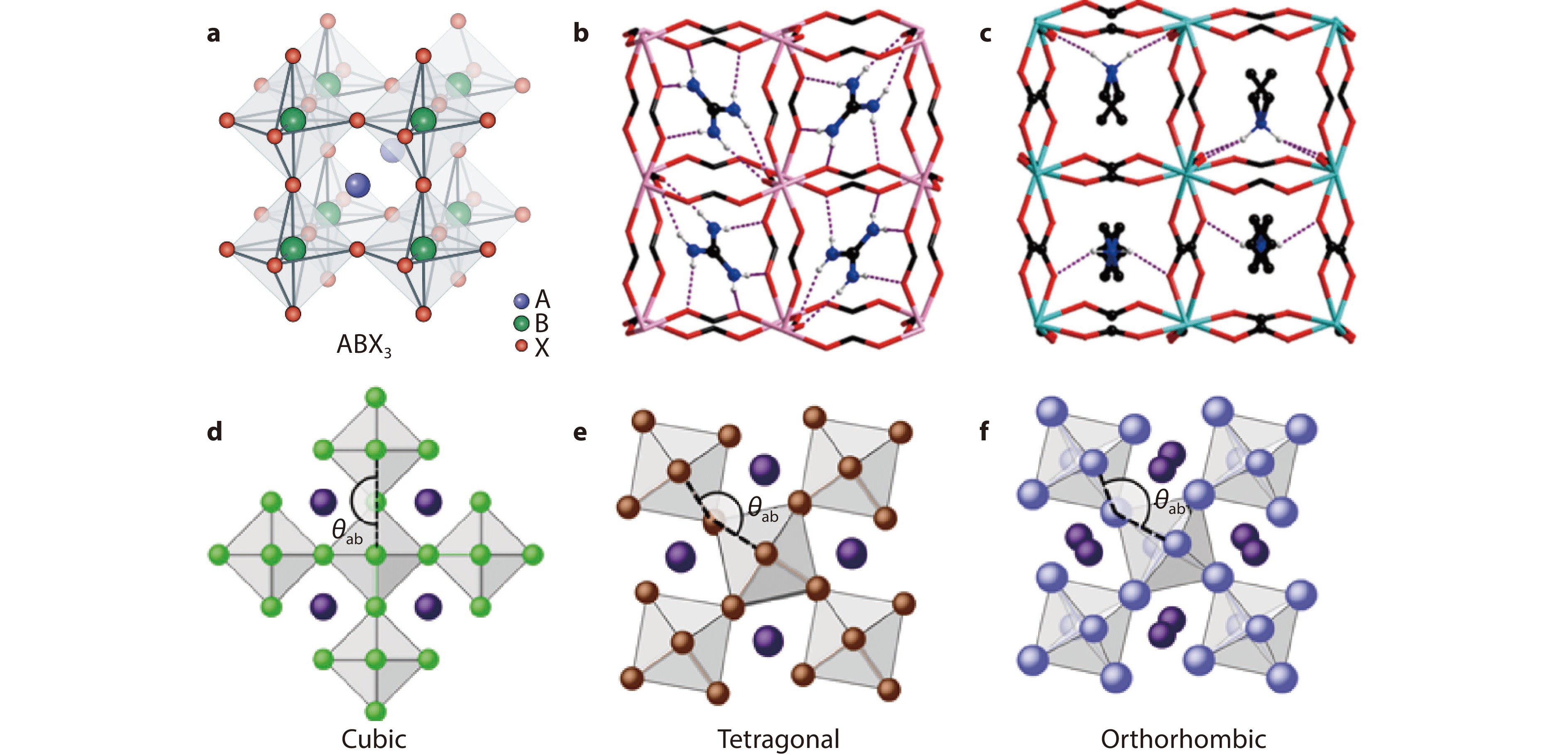
a A general perovskite structure with the stoichiometric formula of ABX3.[21] Copyright 2014, The Journal of Physical Chemistry C. Structural diagram of b (GUA)[Mn(HCOO)3] (GUA-1) and c (AZE)[Mn(HCOO)3] (AZE-2) viewed along the (10"1) direction. Only H atoms bonded with N atoms are shown for demonstration, and the N-H·O hydrogen bonds are represented as dashed lines. Color scheme: Mn, rose or aqua; N, blue; C, black; H, light gray.[30] Copyright 2019, Coordination Chemistry Reviews. Typical crystal phases of ABX3 MHPs including d cubic phase, e tetragonal phase and f, orthorhombic phase. The symmetry descent is related to small coherent displacements of halides, leading to bending of Pb- X-Pb angles with θab= θc = 180°, θab< 180° and θc = 180°, and θab= θc < 180°.[34] Copyright 2017, ACS Nano.
-
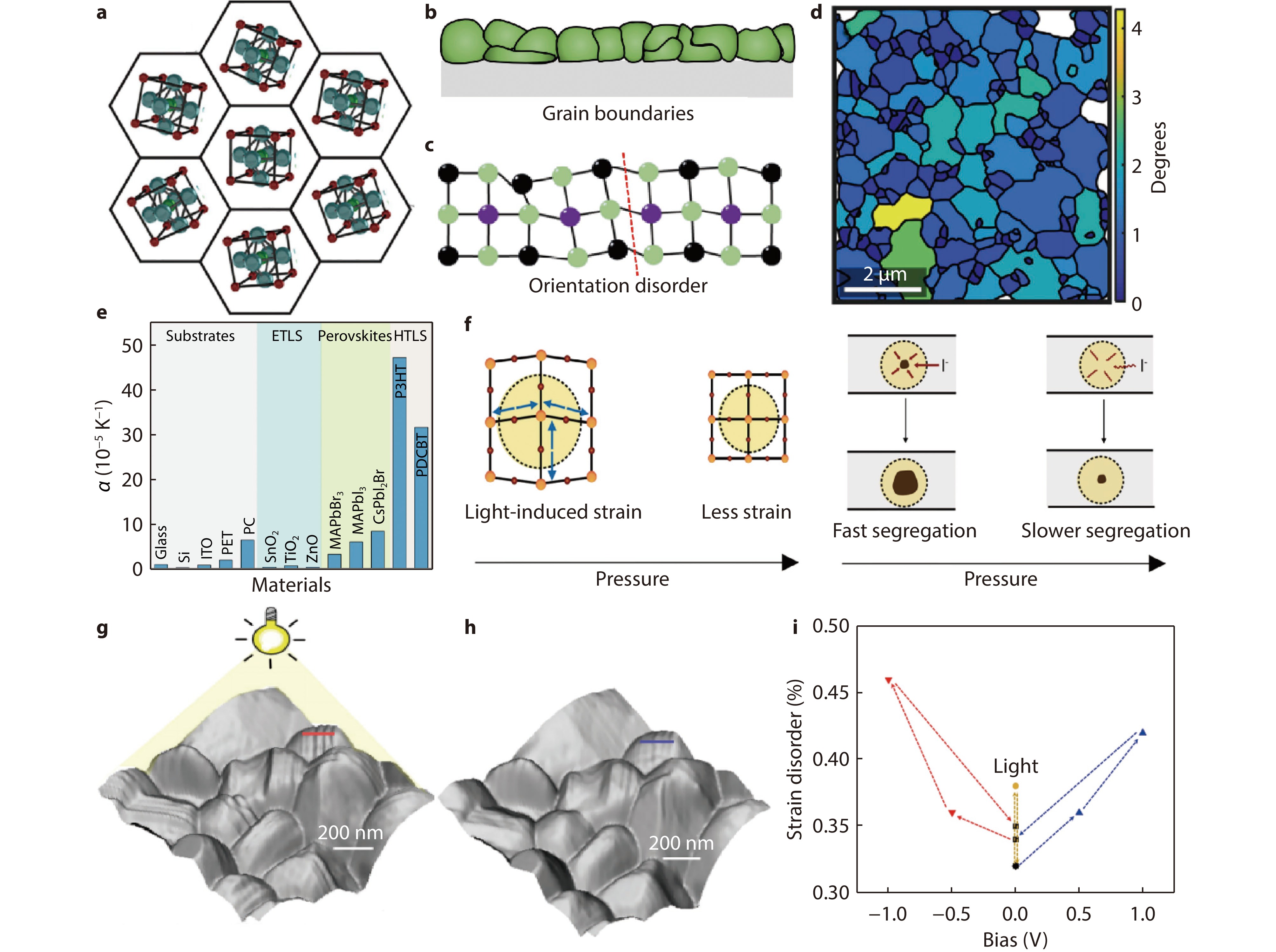
Figure 2.
a Schematic illustration of sub-grain orientation heterogeneity induced stain in CH3NH3PbI3 perovskite films.[37] Copyright 2019, Joule. b Grain boundaries. c The purple spheres are the A-site cations, and the black and green spheres represent metal cations and halide anions, respectively. The red dashed line in c indicates a twin boundary.[38] Copyright 2021, Nature Materials. d Plot of grain orientation spread (GOS) showing grain-to-grain heterogeneity in average local misorientation in the same film.[37] Copyright 2019, Joule. e Thermal expansion coefficients of functional layers in PSCs including perovskites, substrates, ETLs and HTLs.[15] Copyright 2020, Nature Communications. f Illustrations of strain pressure and light-induced strain, which affects the rate of halide segregation in mixed-halide perovskites.[40] Copyright 2020, ACS Energy Letters. Morphological imaging of (FAPbI3)0.85(MAPbBr3)0.15 perovskite film surface g under light, showing distinct corrugated surfaces, and h without light, where the surface is smoother. i The effect of applied electrical bias and illumination on strain disorder in such perovskite.[42] Copyright 2019, Nature Communications.
-
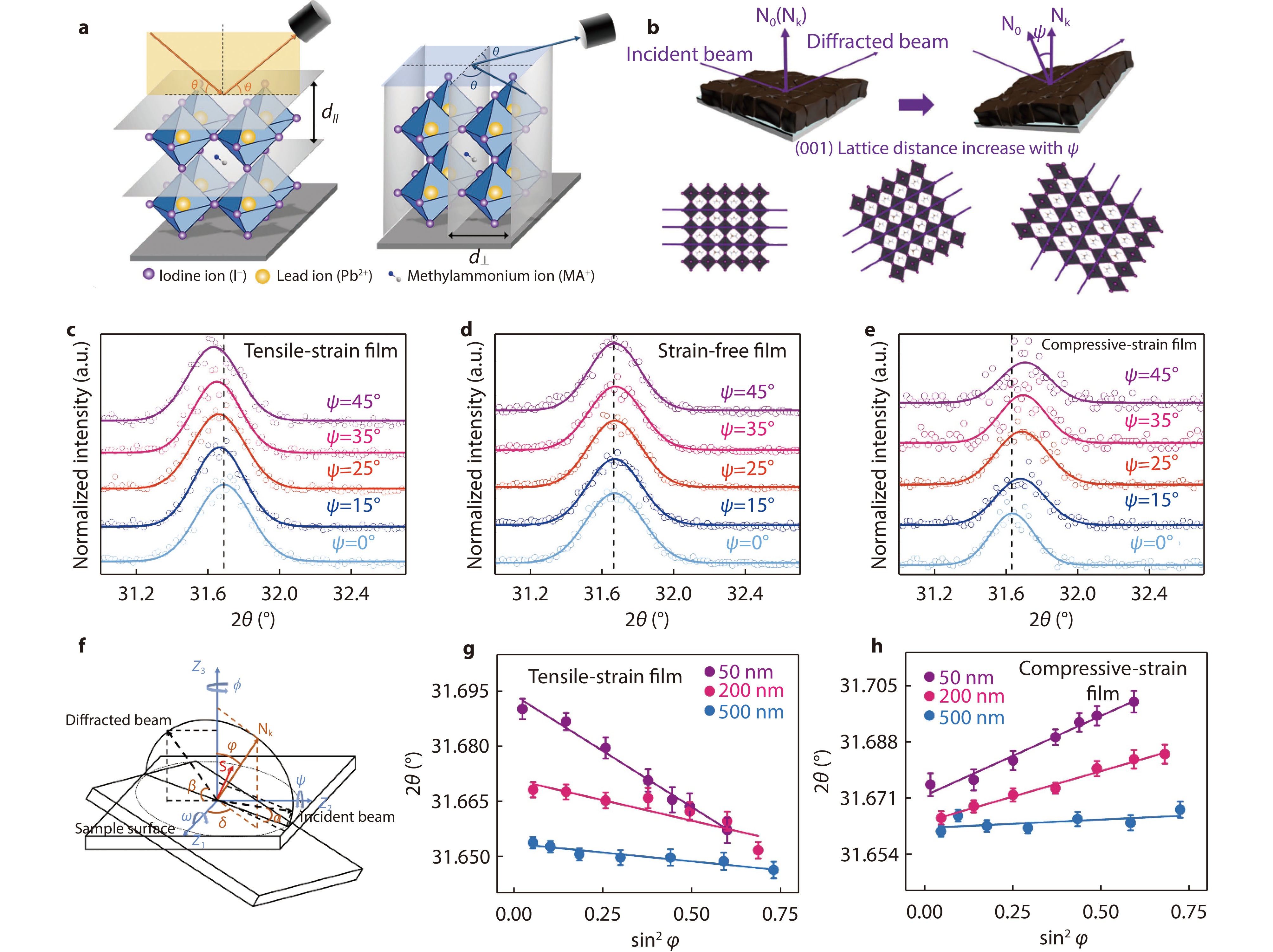
Figure 3.
a The differentiation between out-of- and in-plane diffraction-based characterizations.[13] Copyright 2017, Science Advances. b Illustration of how tilting the instrument angle c allows to obtain difference between the sample normal vector (N0) and scattering vector (Nk). XRD reflections of the same sample at different grazing angles under c tensile strain, d no strain and e compressive strain. f Diffraction geometries of depth-dependent strain distribution measurement. Strain distribution at depths of 50, 200 and 500 nm as a function of sin2φ for the g tensile-strained and h compressive-strained film. The error bar represents the standard deviation of 2θ.[35] Copyright 2019, Nature Communications.
-
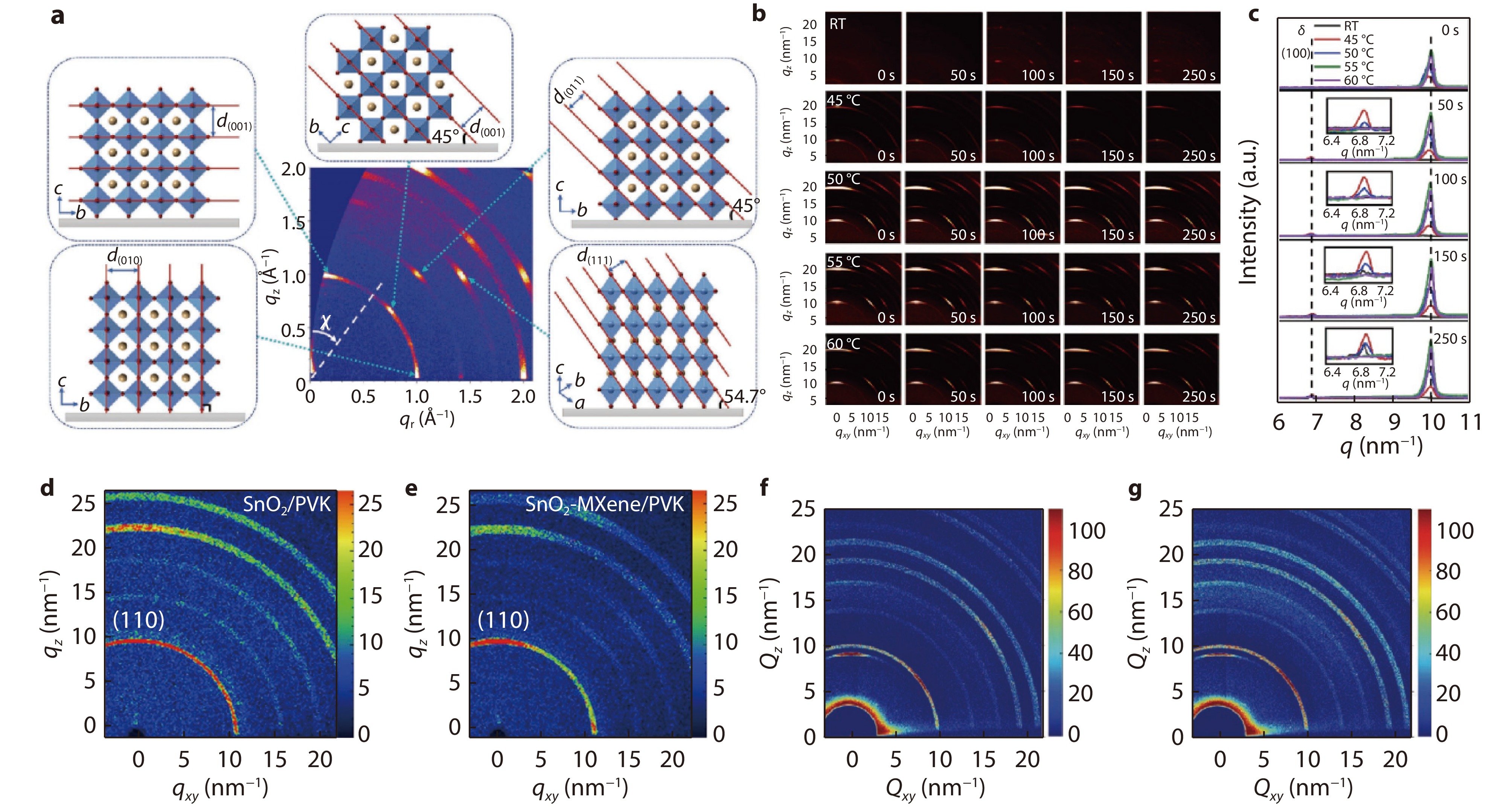
Figure 4.
a A schematic illustration of the GIWAXS pattern obtained from a highly oriented 3D perovskite film.[47] Copyright 2021, Advanced Materials. b Time-varying map of 2D- GIWAXS spectra of perovskite films at different processing temperatures under different annealing time. c Comparison of one dimensional GIWAXS integral at RT-casting (black), 45 °C-casting (red), 50 °C -casting (blue), 55 °C -casting (green), and 60 °C -casting (purple) under different annealing time.[48] Copyright 2020, Nano Energy. GIWAXS patterns of d SnO2/PVK and e SnO2-MXene/PVK film. SnO2-MXene induces oriented growth of PVK.[49] Copyright 2022, Angewandte Chemie International Edition. GIWAXS 2D reciprocal space maps of f control sample and g target sample.[50] Copyright 2022, Advanced Functional Materials.
-
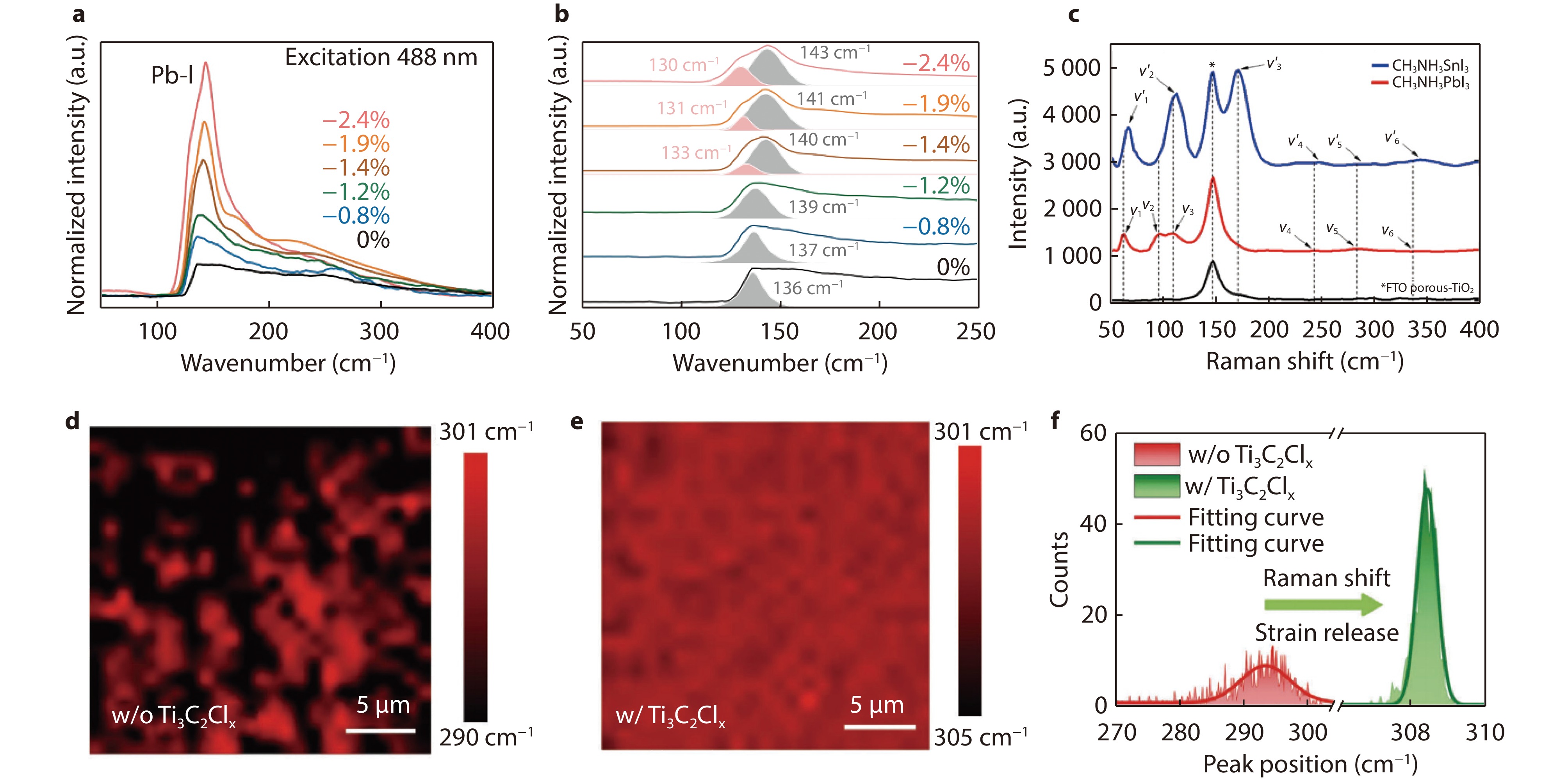
Figure 5.
a Confocal Raman spectra of the epitaxial α-FAPbI3 layer at different strains. b Fitting analysis of the Raman peaks in a.[16] Copyright 2020, Nature. c Raman spectra obtained from pure MAPbI3, MASnI3, and FTO/porous-TiO2 substrate.[51] Copyright 2020, The Journal of Physical Chemistry C. Raman mapping images of CsPbBr3 perovskite films d without and e with Ti3C2Clx MXene, and f the corresponding distribution statistics of Raman peak for different perovskite films.[53] Copyright 2021, Advanced Science.
-
Figure 6.
Cross-sectional TEM image of the interfacial misfit dislocations for a GaSb and b InSb grown on GaAs samples with (2×8) Sb reconstruction prior to growth, respectively.[59] Copyright 2017, Applied Surface Science. c HRTEM image of P-Nb2CTx MXene nanosheet. The inset image shows the corresponding selected area electron diffraction (SAED) pattern.[60] Copyright 2022, Advanced Functional Materials. d The cross-sectional TEM image of device. e,f,g The NBED patterns ([100] zone axis and TEM specimens is FIBed), corresponding with e-f-g point in d, confirming the FAMA hybrid perovskite phase structure transform to nearly pure FA phase from the surface to the bottom of perovskite film according to the larger quadrangle.[35] Copyright 2019, Nature Communications. h SED patterns of triple/cation perovskite corresponding to [001]c zone axis demonstrating the presence of superlattice reflections (white arrows), which are normally forbidden in a cubic Pm3m structure, often assumed for halide perovskite materials, as shown in i. Analyzing SED pattern near [110]c zone axis in j allows to conclude that perovskite has a P4/mbm structure shown in k. Scale bar is 0.5 Å−1.[62] Copyright 2021, Science.
-
Figure 7.
a Schematics of EBSD measurement on CH3NH3PbI3 thin films. b Top-view SEM image and c IPF map generated from EBSD of CH3NH3PbI3 thin film with IPF color key. d Depiction of changes in local crystal orientation along the black arrow in b and c as viewed normal to the sample.[37] Copyright 2019, Joule.
-
Figure 8.
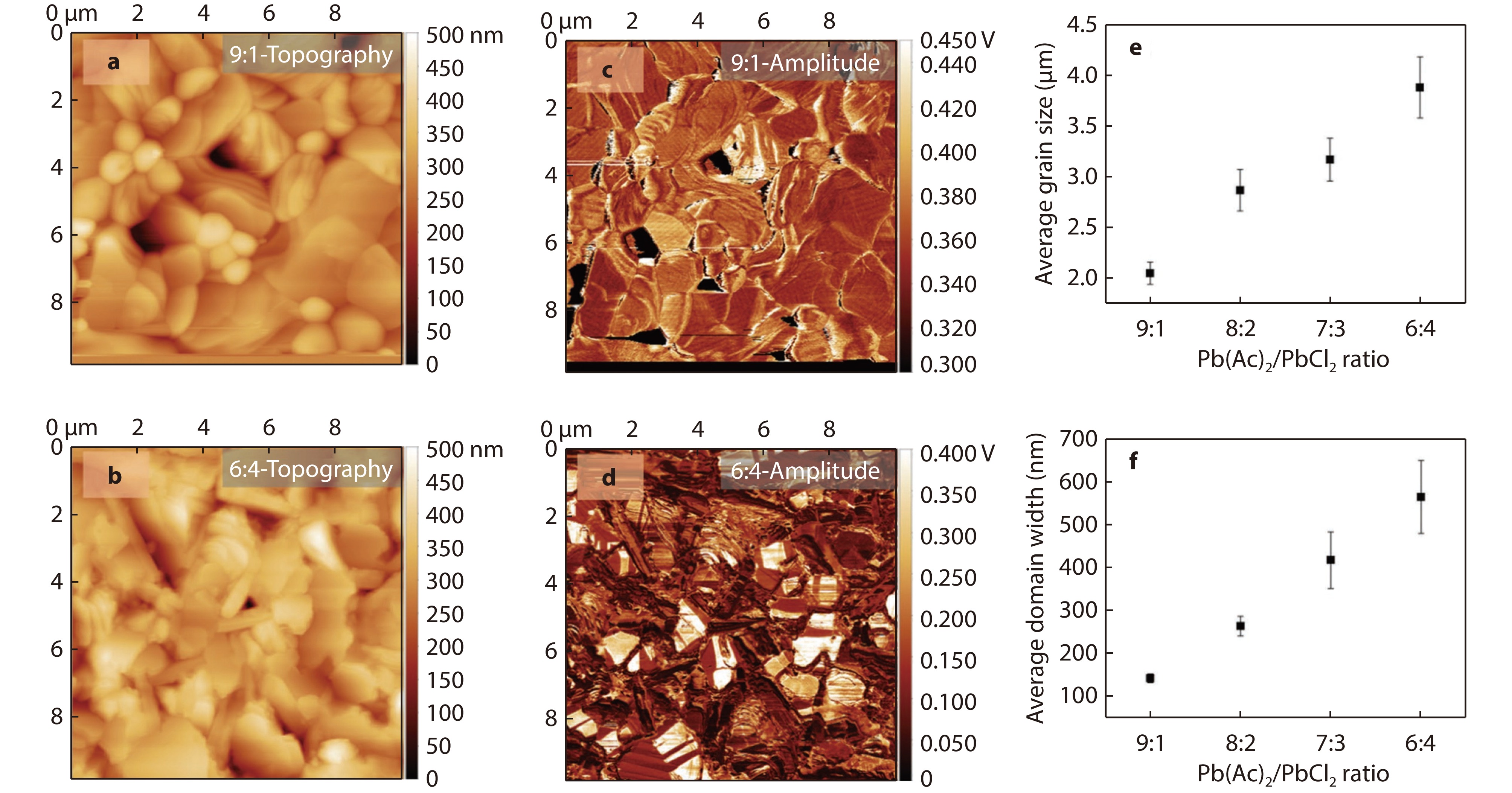
Topography and PFM amplitude images of MAPbI3 thin films with Pb(Ac)2/PbCl2 ratios of a, c 9:1, and b, d 6:4. e Average grain size and f domain width profiles of MAPbI3 thin films with different Pb(Ac)2/PbCl2 ratios.[64] Copyright 2022, Advanced Energy Materials.
-
Figure 9.
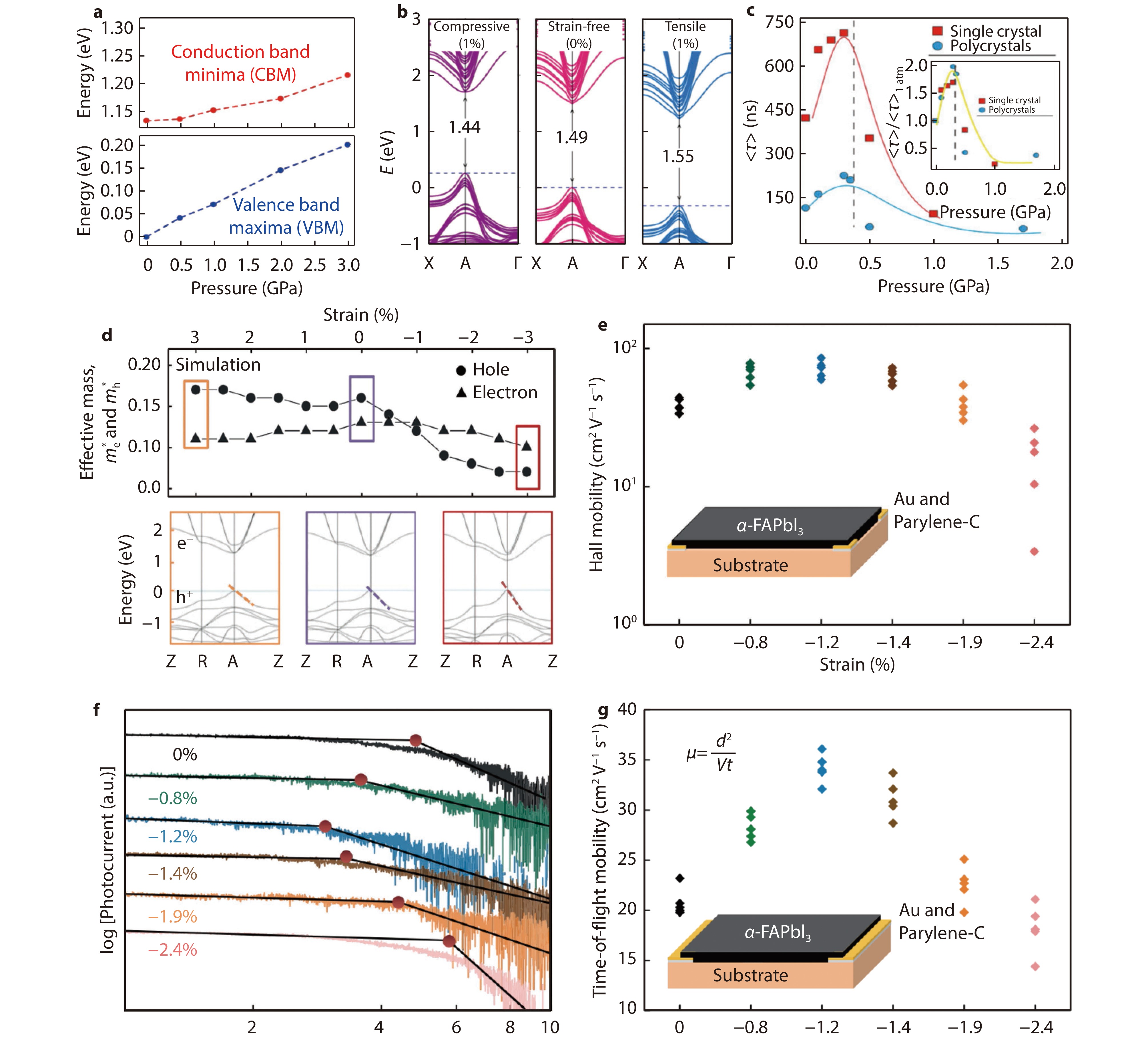
a Modification in energy of CBM and VBM.[9] Copyright 2021, National Science Review. b Calculated band structures under biaxial tensile, zero, and compressive strains from first-principle density functional theory (DFT)-based approaches.[35] Copyright 2019, Nature Communications. The band structure alignment is made by using the vacuum energy level as reference. c Pressure dependence of the mean carrier lifetime, for both MAPbI3 single-crystal and polycrystal samples. Peak values in carrier lifetimes of MAPbI3 were observed at 0.3 GPa. (c Inset)[65] Copyright 2016, Proceedings of the National Academy of Sciences. d Calculated effective masses of the carriers at different strains, and electronic band structures under three strain levels (3%, 0% and −3%). e Hole mobilities by Hall effect measurements. f Transient photocurrent curves of the epitaxial α-FAPbI3 under different strains. g Plots of calculated carrier mobilities as a function of the strain magnitudes.[16] Copyright 2020, Nature.
-
Figure 10.
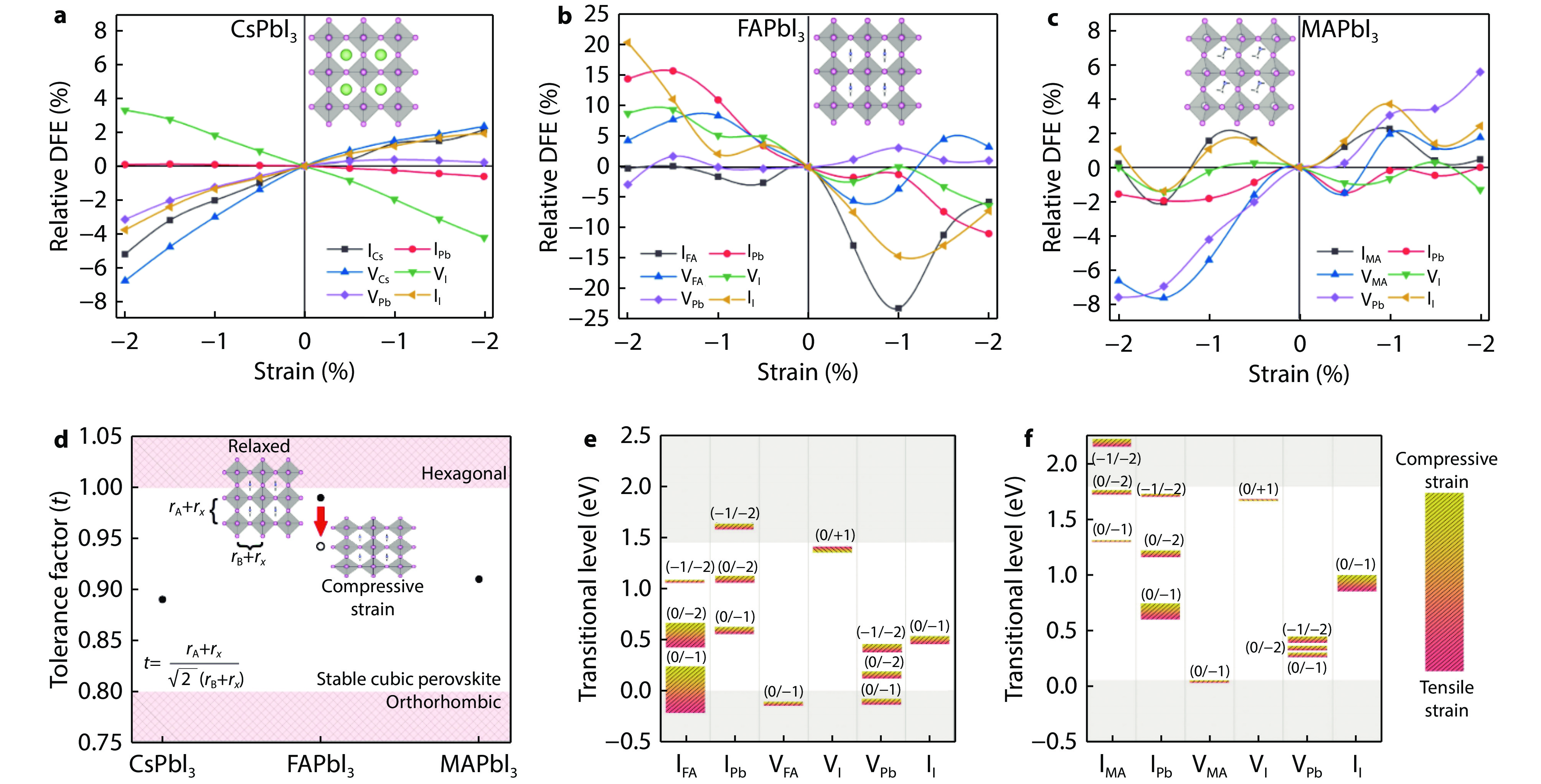
The dependence of the defect formation energies (in eV) on the lattice strain and defect formation energy of the perovskites for different growth conditions. The relative DFE with respect to the strain for selected neutral intrinsic defects (IA, IPb, VA, VI, VPb, and Ii) in a CsPbI3, b FAPbI3, and c MAPbI3 perovskites under moderate conditions. The negative percentage value indicates a compressive strain while the positive percentage value refers to a tensile strain along the out-of-plane direction throughout the study. d Schematic representation of strain-induced tolerance factor adjustment of FAPbI3. Herein, rA, rB, and rX represent the radii of A-site molecule, B-site metal, and X-site halide in ABX3 perovskites, respectively. In addition, rA+rX is a space-diagonal length. The change in the tolerance factor of FAPbI3 is enlarged to show the influence of the strain. The charge transition energy levels of selected intrinsic defects in e FAPbI3, and f MAPbI3. The influence of lattice strain on the transition levels is shown by the color gradient. The strain is varied from −2% (compressive) to 2% (tensile).[67] Copyright 2022, Nano Research.
-
Figure 11.
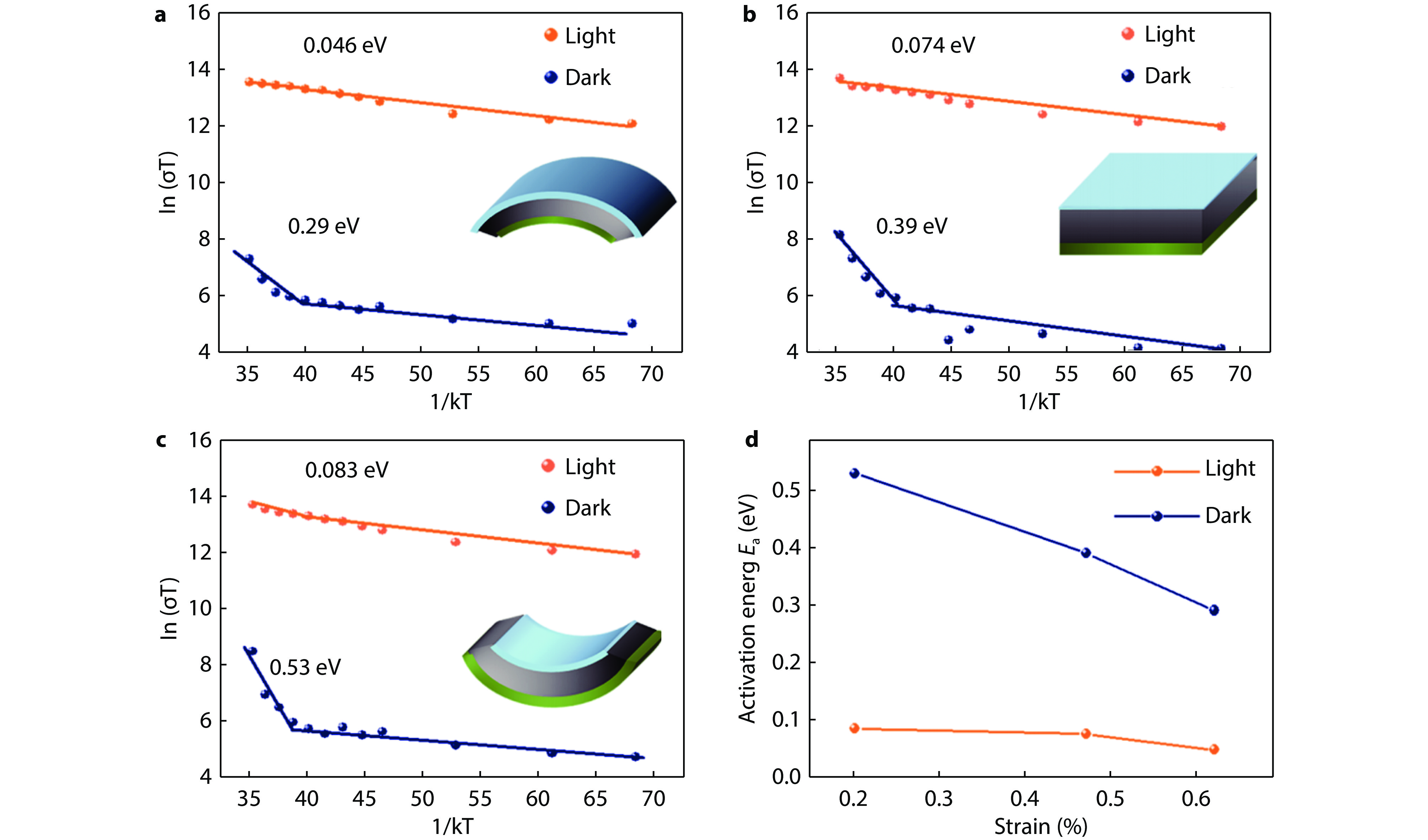
Ion migration properties of MAPbI3 films at different strains. a-c The temperature-dependent conductivity of a the convex film, b the flat film, and c the concave film. Inset: Schematic diagram of the samples. d Variation of the activation energy of ion migration as a function of the strain in the MAPbI3 films.[13] Copyright 2017, Science Advances.
-
Figure 12.
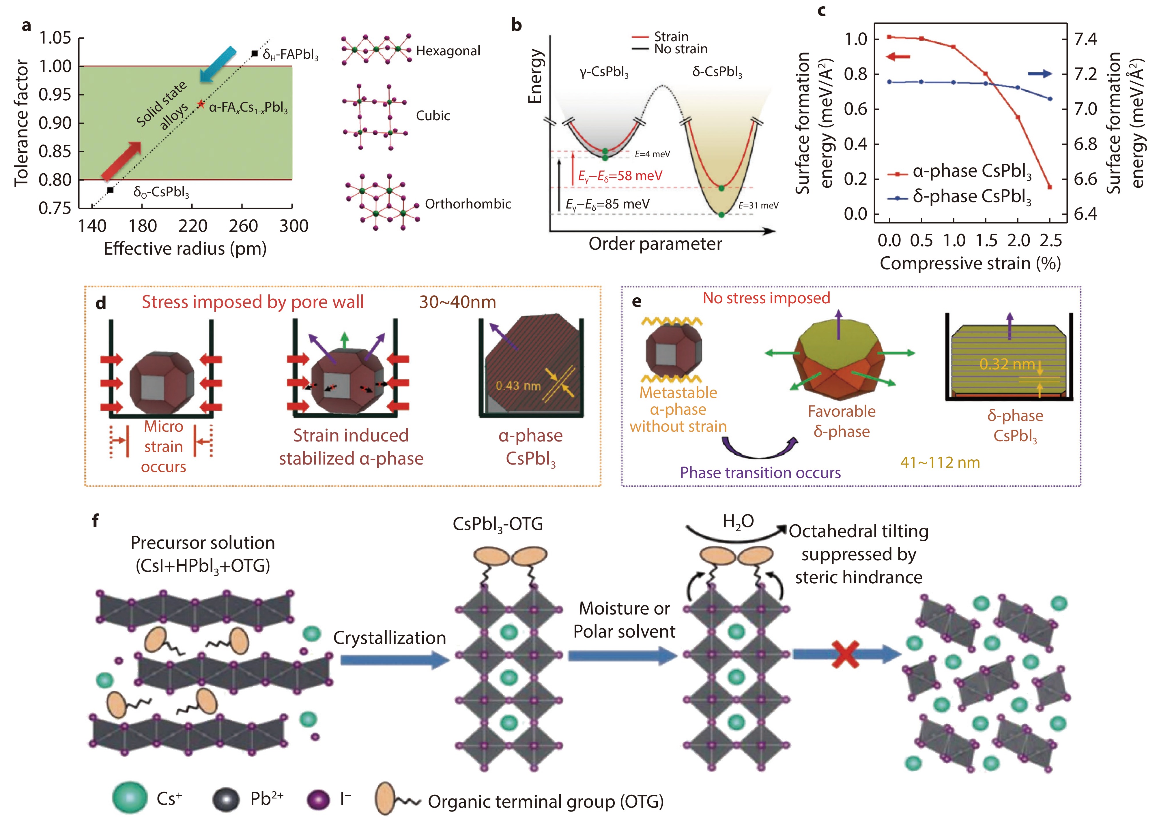
a Correlations between tolerance factor and crystal structure of perovskite materials.[72] Copyright 2016, Chemistry of Materials. b The schematic diagram for the relative stability of the black phase and yellow phase with and without biaxial strain.[12] Copyright 2019, Science. c Dependence of surface formation energy on the imposed compressive strain obtained through a theoretical calculation.[75] Schematic describing the polycrystalline growth mechanism of d α-phase CsPbI3 perovskite in 41 nm pore-sized anodized aluminum oxide (AAO) template and e δ-phase CsPbI3 perovskite in 112 nm pore sized AAO template. Copyright 2019, Small. f Mechanism of the OTG-induced phase stabilization of CsPbI3 perovskite. [76] Copyright 2019, Advanced Materials.
-
Figure 13.
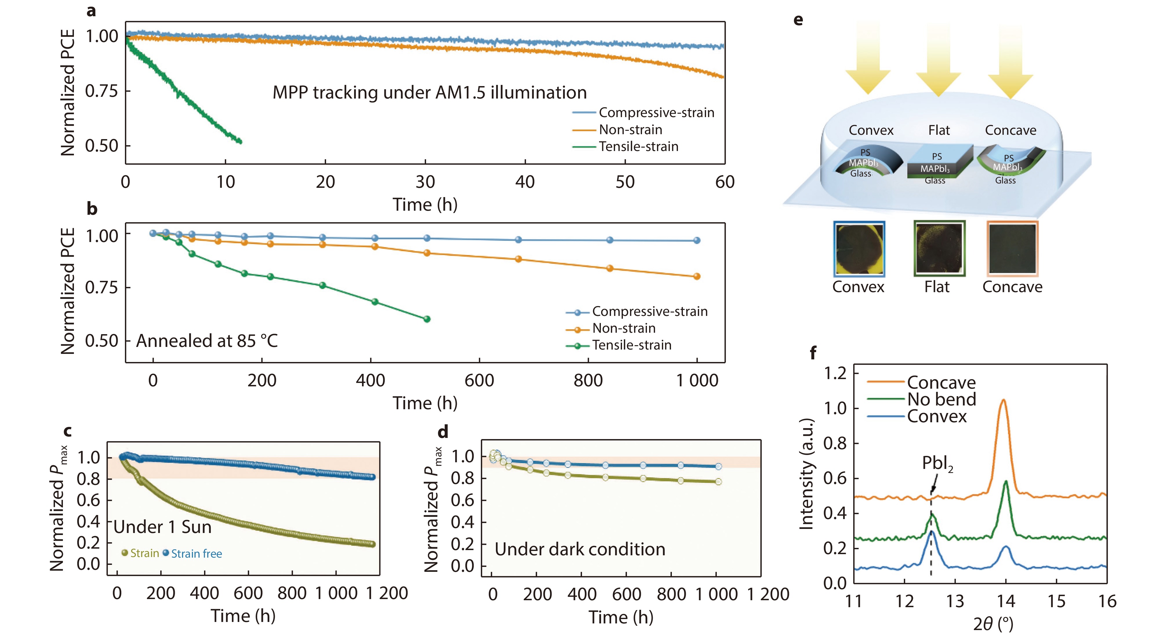
a Evolution of normalized PCEs under MPP tracking and continuous simulated solar illumination (100 mW cm−2). b Evolution of normalized PCEs of PSCs kept at 85 °C in a nitrogen atmosphere. The device stability tests under continuous white LED illumination.[15] Copyright 2020, Nature Communications. c The light intensity was adjusted in a way that the Jsc matched the ones under a solar simulator. d The device stability tests in the dark.[77] Copyright 2022, Joule. Strain impact on perovskite film stability. e Schematic diagram for the experimental setup of the films with different strains and photographs of the films with different strains after 500 h illumination. f Out-of-plane XRD of the three films in a. [13] Copyright 2017, Science Advances.
-
Figure 14.
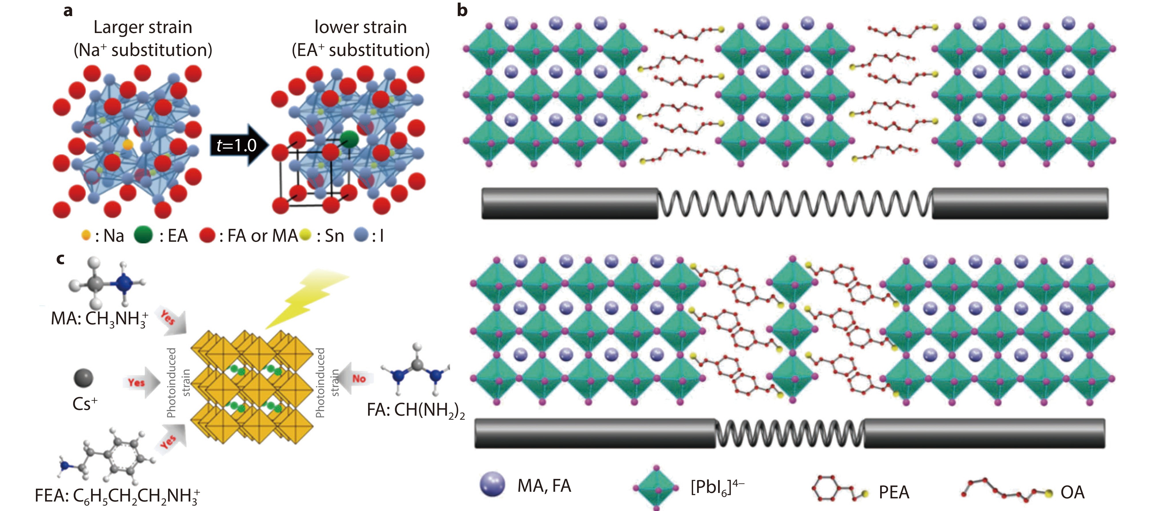
a Schematic diagram for the adjustment of A-site in FA0.75MA0.25SnI3 perovskite to reduce lattice strain.[78] Copyright 2019, ACS Applied Materials & Interfaces. b Schematic describing the residual stress relaxation with soft and stiff structural subunits.[79] Copyright 2019, Advanced Materials. c Schematic diagram for the adjustment of A-site in perovskite to reduce lattice strain.[80] Copyright 2019, Journal of Materials Chemistry A.
-
Figure 15.
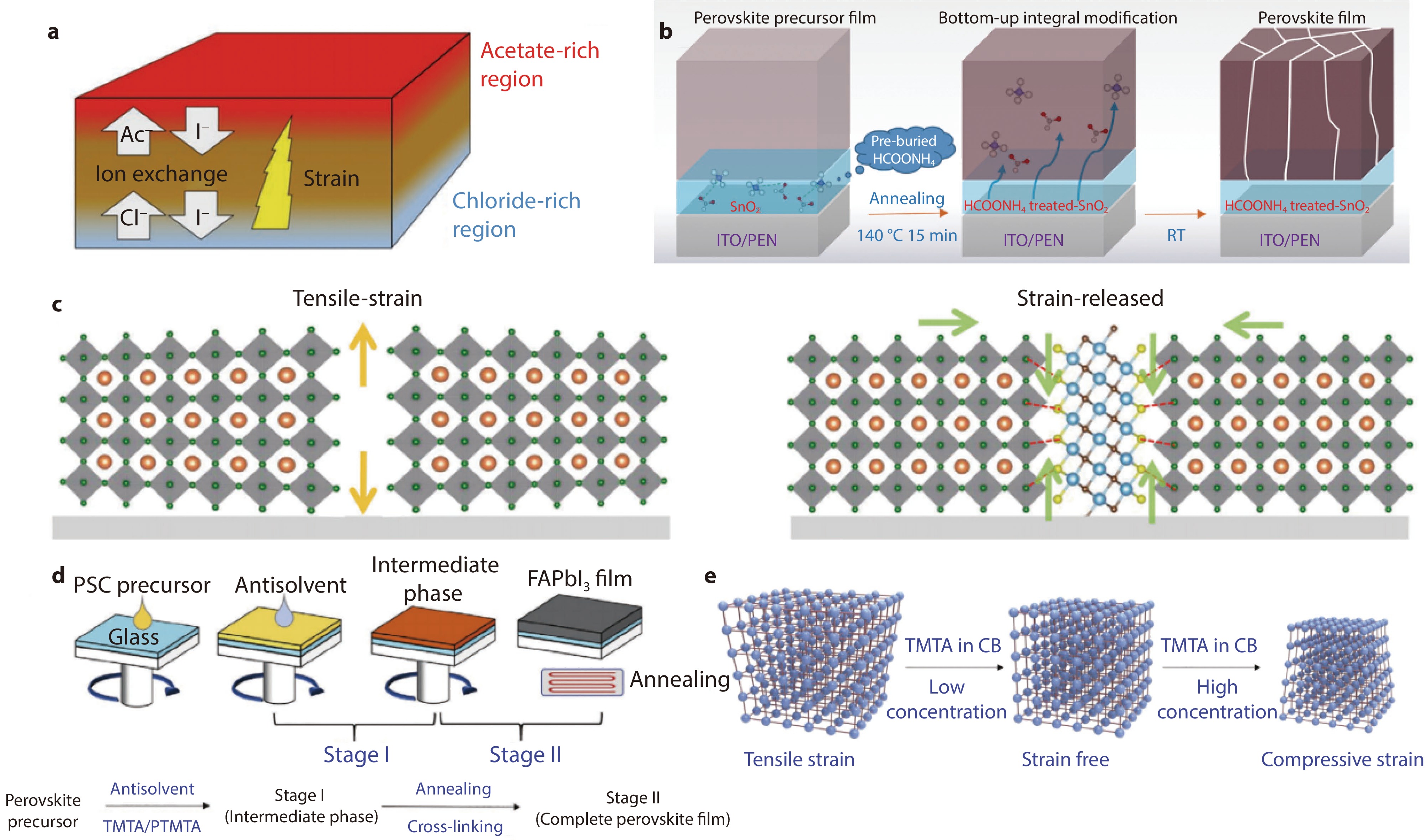
a Illustration for strain mechanism.[64] Copyright 2022, Advanced Energy Materials. b Schematic illustration for the functionalization process of pre-buried HCOONH4 additive.[83] Copyright 2022, Advanced Materials. c Schematic diagram for the residual strain in pristine CsPbBr3 grains, schematic diagram of released strain in the reinforced CsPbBr3 grains with Ti3C2Clx MXene.[53] Copyright 2021, Advanced Science. d The schematic representation for the tensile strain state of the control PSC film regulated by CSRC method. e Schematic illustration for the two stages of perovskite formation kinetic with TMTA-CSRC treatment.[85] Copyright 2021, Advanced Materials.
-
Figure 16.
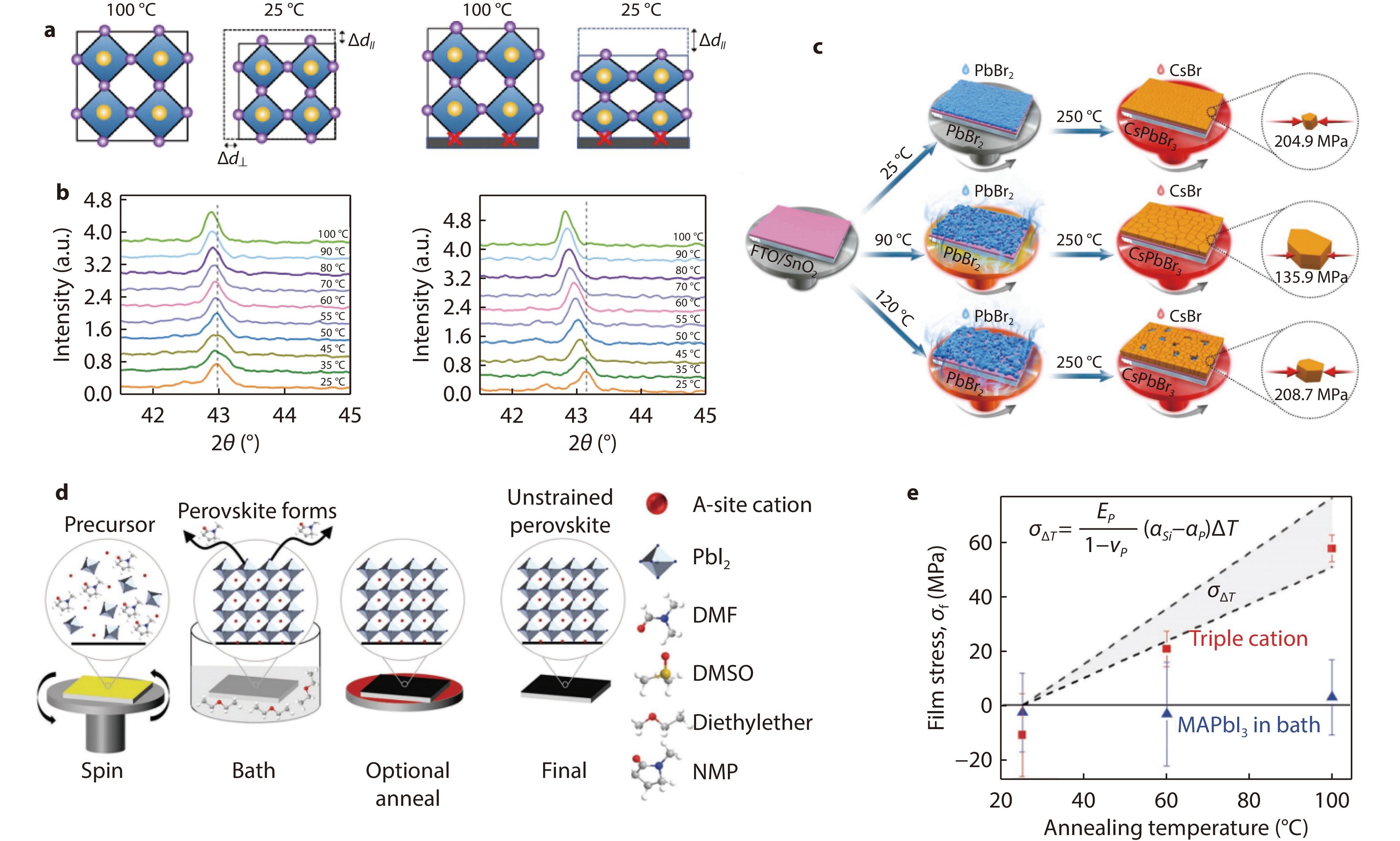
a The perovskite forming at 100°C contracts vertically and laterally during cooling without and with substrate. b In-situ out-of-plane XRD patterns of scraped powders and annealed films at different temperatures.[13] Copyright 2017, Science Advances c Diagram of converting PbBr2 into perovskites at low, intermediated and high temperatures as well as compression strains of perovskites.[88] Copyright 2020, Nano Energy. d Schematic illustration for the film formation during perovskite film formation and the effect on molecular structure for antisolvent processing of perovskite with using a bath conversion after spin-coating. e Measured stress for CsMAFA (red) formed at 25, 60 and 100 °C. Measured stress for MAPbI3 (blue) formed at room temperature and with a post anneal at either 25, 60, or 100 °C, showing low stress values in all cases since the perovskite was fully converted before annealing.[39] Copyright 2022, Advanced Energy Materials.
-
Figure 17.
a The calculated net average stress in perovskites within the structures consisting of ITO/TiO2/perovskite/PDCBT as a function of PDCBT spin-coating temperature.[15] Copyright 2020. Nature Communications. b Optimized 2D/3D perovskite processing procedures. c GIXRD spectra at different tilt angles for the PCBM-2 h thin film. d Residual tensile strains of PEA2PbI4 films under different preparation technologies. e Schematic diagram for strain compensation caused by covering PCBM. f Magnified diffraction peaks of (002) plane from 2D perovskite.[90] Copyright 2020, Advanced Energy Materials.
-
Figure 18.
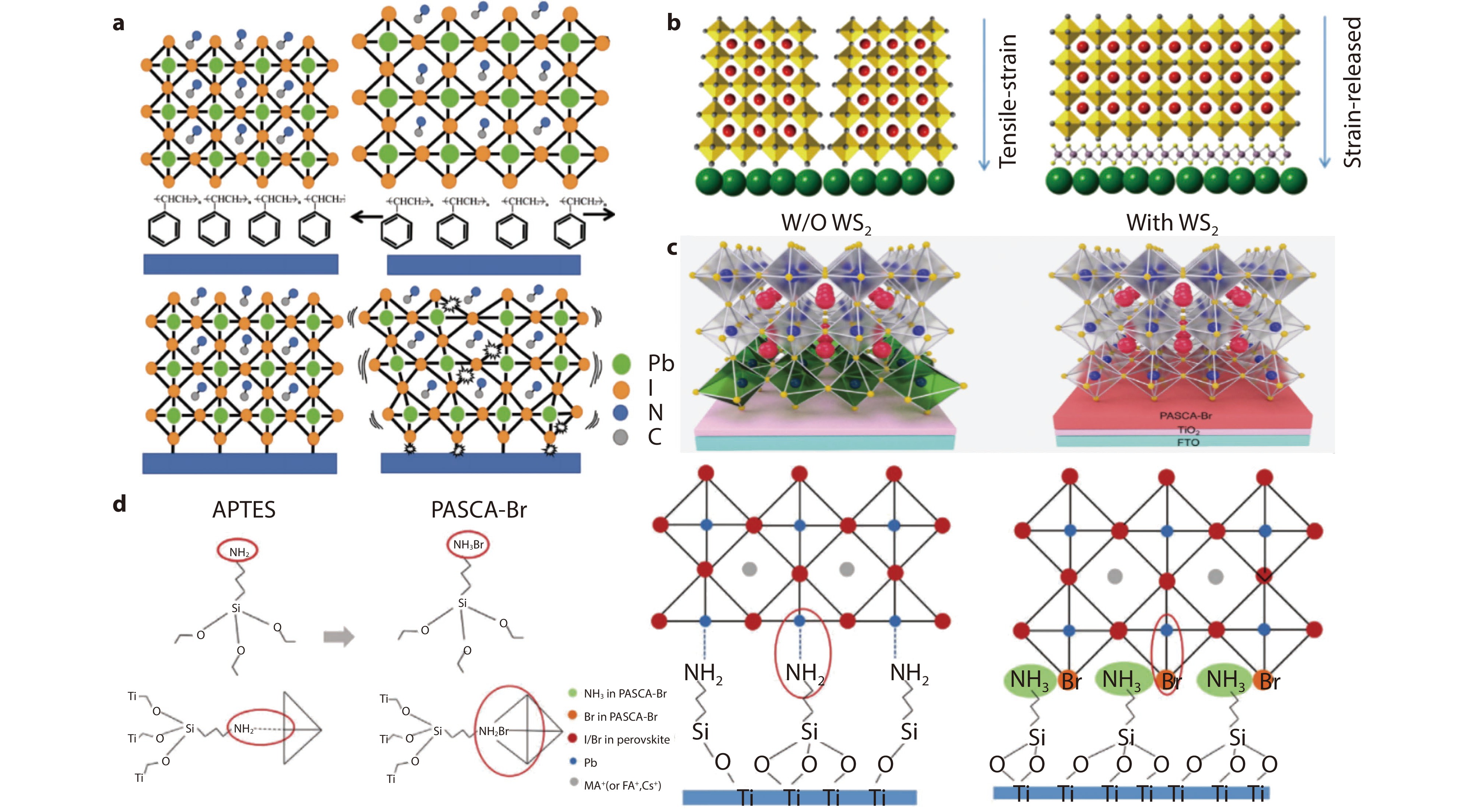
a Schematic illustration for the PS buffer layer to release the strain: as-prepared perovskite films with PS, annealed perovskite films with PS, as-prepared perovskite films without PS, and annealed perovskite films without PS.[91] Copyright 2019, Advanced Functional Materials. b Schematic diagram for the residual strain distribution in CsPbBr3 grains with and without WS2 interlayer.[92] Copyright 2020, Angewandte Chemie International Edition. c A schematic of perovskite crystals at the interface. d Protonated amino terminals (R-NH3Br) and lattice structure of APTES and PASCA-Br modified interfaces.[93] Copyright 2020, Advanced Materials.
-
Figure 19.
a GIXRD spectra of control and target perovskite films with different instrumental tilt angles ψ values in the depth of 200 nm. Macroscope residual strain distribution analysis by linear fitting of 2θ-sin2ϕ for control and target perovskite films. b Microstructure of Pb-I frame plane perpendicular to the b-axis, where two Pb atoms bind with the BMI.[50] Copyright 2022, Advanced Functional Materials. c Illustration of as-prepared CsPbI2Br solar cells with the structure of ITO/SnO2/perovskite/J71/spiro-OMeTAD/MoO3/Ag, molecular formula of J71 d, Crystal mechanics model of control and CsPbI2Br/J71.[98] Copyright 2022, Chemical Engineering Journal. e Schematic representation of surface reconstruction process after CMAI (IPA) and CMAI (CF) treatment.[100] Copyright 2022, Nano Energy.
-
Figure 20.
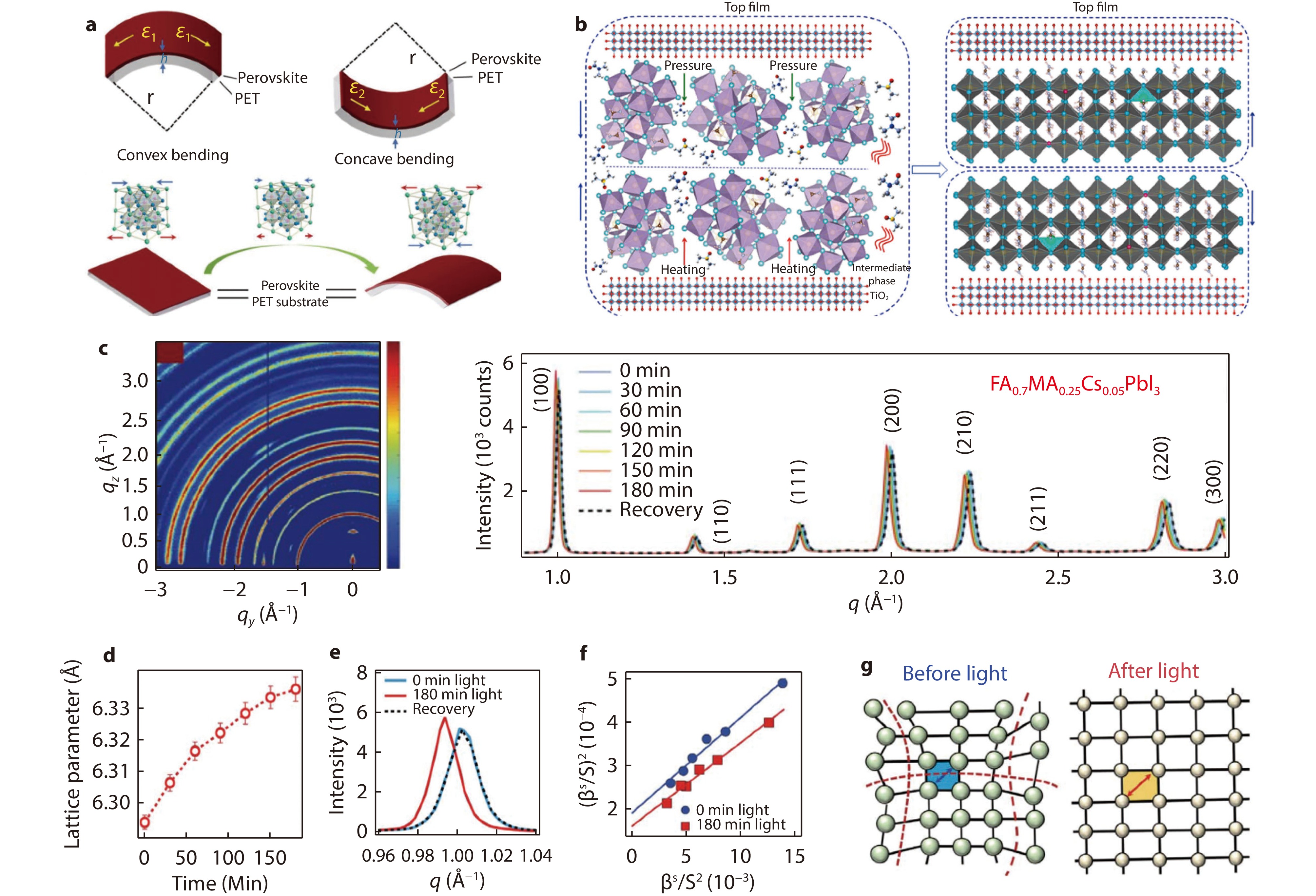
a Schematic diagrams for convex, concave bending and lattice strain changes during a convex bending process.[101] Copyright 2020, Journal of Materials Chemistry C. b Schematic diagrams for convex, concave bending and lattice strain changes during a convex bending process.[102] Copyright 2020, Nano Energy. Light-induced lattice expansion and structural analyses. c A typical synchrotron diffraction pattern (left) and the line cut of GIWAXS maps (right) for FA0.7MA0.25Cs0.05PbI3 (cubic phase) thin films under various illumination times and the recovery spectra obtained after the films were kept in the dark for 30 min. qy, vector along in-plane direction, and qz, vector along out-of-plane direction in reciprocal space with respect to the substrate. d Lattice constant as a function of illumination time. e Peak change before and after 180 min of illumination and recovery in the dark. f Linear fit of integral-breadth analysis using Halder-Wagner plots, where b is the integral breadth of the diffraction peak and S is defined as S = q/2p. g Schematic illustration for the crystal structure change before (local distortion) and after illumination (lattice expansion).[41] Copyright 2018, Science.

 Yuanyuan Zhao is an academic professor in the College of Mechanical and Electronic Engineering at Shandong University of Science and Technology (Qingdao, China). She received her Ph.D. from Ocean University of China. Her research interests cover all-inorganic perovskite solar cells, electrocatalytic hydrogen production.
  Qunwei Tang is a senior Professor in the College of Chemical and Biological Engineering at Shandong University of Science and Technology. He is the dean of Institute of Carbon Neutrality and youth editor for eScience journal. His research interests cover perovskite solar cells and triboelectric nanogenerators. Up to date, he has published more than 350 papers in international journals such as Angewandte Chemie International Edition, Advanced Materials and two professional books. He has been listed in Chinese Most Cited Researchers, Career Scientific Impact (2021, 2022), World’s Top 2% Scientists (2021, 2022). He also won the second prize of Guangdong Province Science and Technology Award (China), the first prize of Yunnan Province Science and Technology (China).
 DownLoad:
